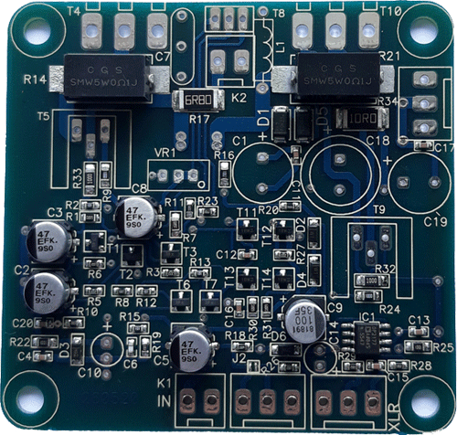
PCB design
More and more companies are identifying and understanding the positive impact of contracting for manufacturing services
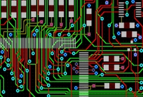
DESIGN OF PRINTED CIRCUIT BOARD
These includes:
- Time-to-market is sharply reduced
- management’s time is free to concentrate on marketing and R&D
- using immediate resource to address engineering issues/concerns for manufacturability
- Money is saved by reducing overhead – no capital outlay is required
The key word in design as well as in development is trust. In layout design partners has to exchange valuable information for design goal. This includes
- correct schematic for layout design
- board(s) dimensions
- list of all components included in design
- number of layers
- technology for assembling: SMD one side or both?
- estimating time for layout design
- output format of files and documentation
PIt is necessary to analyze all design aspects, and fulfill details through design to complete manufacturing documentation. Design has to be verified in suitable fazes, supply with all technological parameters and established way off communications with check points before layout is ready for board manufacturing. We consider customer’s suggestions and requests at all times.
Experience shows us that there is strong possibility for partnership on a design projects concerning close working together on specific project.
Technical side is having the same PCB design software and PC platform.